 Iron Oxide Beads Coated with Silica There are different materials and metals which we found on this earth. Some of them are also present on other plants in this universe. Some of them are located on the earth in great amount and some are having very less percentage of presence. But silica is the one that is considered as the second most available material in this universe. And on earth, this is located in great amount. Now the silica beads are announced for the market. These beads have also started to come in different forms such as iron oxide coated ones and magnetic ones.
0 Comments
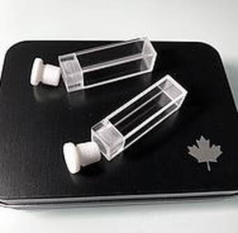 10mm Quartz Cuvettes with Stoppers If you are working at a laboratory, then you must know how important it is to use the cuvettes. These are the containers that are used in great numbers to hold the samples and chemicals. These containers play a very vital role at different labs where spectroscopic analyses are done frequently. To perform these tests, holding the samples safely is a very vital work. Once these samples are not there, these tests cannot be done. The use of the 10mm quartz cuvettes with stoppers can really help you store and hold these chemicals and samples in the safest possible manner. As these cuvettes are equipped with the stoppers, the chemicals inside these containers will not fall down or spill on the lab’s surface. Cuvettes are made from different materials such as quartz, plastic, glass, etc. But the quartz cuvettes have really managed to take the front seat when it comes to the laboratory tests.
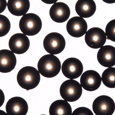
 Magnetic Silica Nanoparticles There is a wide range of nano particles used these days. These nano particles are used for a wide range of applications and purposes. Especially to do a wide range of tests properly and to draw accurate reading and result, these nano particles are used. You can say that the use of these nano particles have really managed to make these tests accurate, proper, safe and convenient for us. Magnetic silica nanoparticles are the ones that are best known for their big surface area as well as ease to function. These nano particles are also biocompatible in nature. And due to this reason, they are also used for the biomedical applications and processes in great numbers. All these properties such nano particles have are making them the right choice for the drug delivery systems and applications. As silica is the most commonly found material in this universe and on the earth it is located abundantly, the nano particles made from this material are also in great demand these days.
 Iron Oxide Beads Coated with Silica Silica is the next most available material in this universe. This material is also located on the earth in great amount. And now this material is also used to coat the iron oxide nano particles. When you have the right kind of nano particles to use, the test results can come accurate even at the first instance. Before, to get accurate test results several tests used to be done. But things have changed a lot once these nano particles have started to invade the market. If you are looking for the best quality iron oxide beads coated with silica, then you have come to the right place!
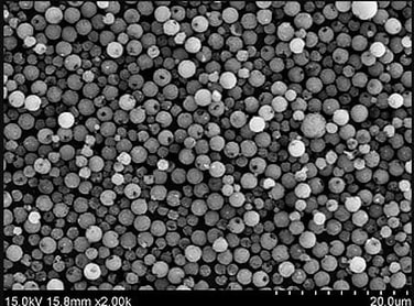
 Poly (Methyl Methacrylate) Microspheres For a wide range of applications and tests, we need the nano particles these days. These are also called as the microspheres and they are used in great numbers and different forms these days to conduct a wide range of tests and experiments. When you are doing these tests, you are also expecting to receive accurate outcome. Before this used to be very tough and after doing several tests, scientists and lab technicians used to receive right result. But the use of the nano particles has really changed the whole scene.
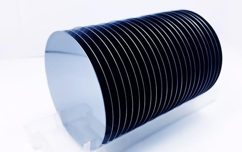 Prime-Grade 4 Inch Silicon Wafer Most of us out there have used the silicon wafer and we don’t even know about this. Now you might be thinking that when you have used this material and how. Well, the electronic items that we are using on a daily basis are the items for which this material is used. To make the functions of these electronic items safe and convenient these silicon wafers are used for them in great numbers these days. This material is primarily used to make the semiconductors. And these are the items that you can easily found with most of the electronic items and applications that we use on a daily basis these days. Without these electronic items, our daily life can really suffer. So these items are very vital for us. And the use of the prime-grade 4 inch silicon wafer has really managed to make the use of these electronic items safer and convenient.
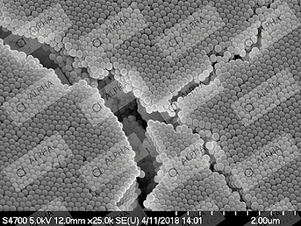
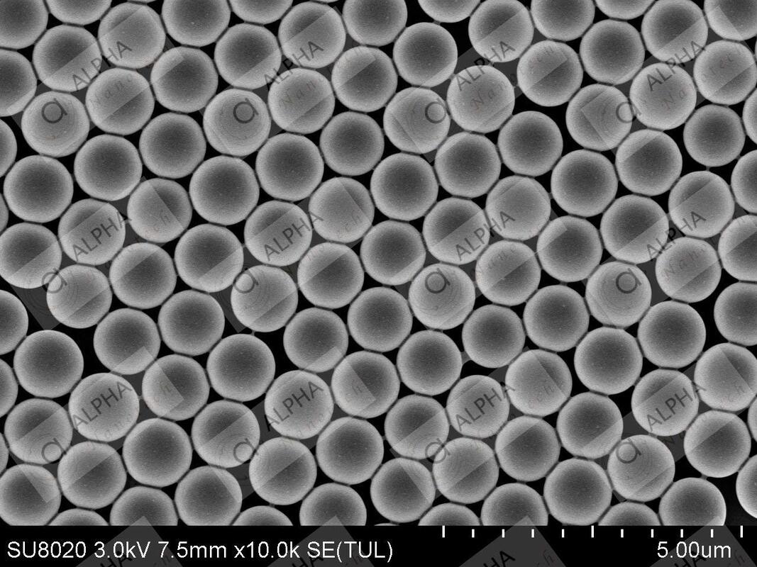 Colloidal Polystyrene Nanoparticles 1μm For a wide range of applications and tests, we are taking help of the nano particles these days to receive accurate outcome. Before several tests were done to receive accurate result and that used to be a very tedious process. But the availability of the nanoparticles these days has really managed to change a whole lot of things. These nano particles have really made the tests with applications look easier, safer and accurate.
There is a wide range of materials and substances that we are using these days to make our life simpler and safer. There is also a wide range of electronic items that we using at our homes, offices and other places. But do you really know that how we are using these items safely. There are different components assigned or installed for these items so that they can be used and operated safely and no issues can arise. When it comes to the electronic field, the use of the silicon wafer seems to be very apparent. These wafers come in different sizes and shapes and used for a wide range of electronic applications and devices to make their usage safe enough! These wafers are also great on the use when it comes to the cell growth and chemical deposition. These are made from the silica substrates and known as the silicon substrates which are coated very uniformly with the help of SiO2 layers which are thermally grown ones. If you are looking for the top quality prime-grade 4 inch silicon wafer, then you have come to the right place! 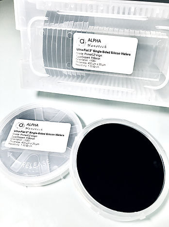 Prime-grade 4 inch silicon wafer
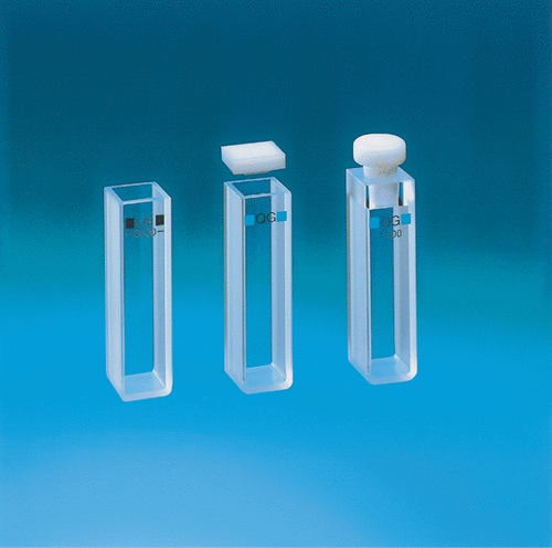 Quartz Cuvettes with PTFE Caps Quartz Cuvettes with PTFE Caps Picking a privilege cuvette for UV VIS range assessments can be basic for research offices utilizing. Not all cuvette materials or types will work for every examination, so some fundamental data is significant for the right decision.
Here we hope to help you with improving appreciation of critical factors to consider while picking an UV-VIS cuvette. Coming up next is a video for some major cuvette types. A Ultraviolet quartz cells with PTFE screw caps and septa is a little chamber like holder with straight sides and a traffic circle or square cross-section. They are ordinarily fixed toward one side and have an additional cap to seal the far edge. Standard cuvettes are all around square or rectangular in cross-portion to keep an essential separation from refraction antiquated rarities. What is a cuvette used for? A cuvette is a touch of exploration focus vial that is used to hold tests answers for spectroscopic examination, where a light outflow is experienced the model inside the cuvette to evaluate the absorbance, movement, fluorescence power, fluorescence polarization, or fluorescence lifetime of the model. This assessment is done with a spectrophotometer. Cuvettes are created utilizing glass, plastic, or optical-grade quartz. Plastic cuvettes have the potential gain of being more reasonable and nonessential and are habitually used in speedy spectroscopic tests. Quartz cuvettes with PTFE caps are used when characteristic solvents are incorporated, which have higher impediment appeared differently in relation to plastic sorts. At the point when everything is said in done, quartz and glass cuvettes show more significant straightforwardness and precision of assessment, and they can be re-used numerous events over plastic cuvettes 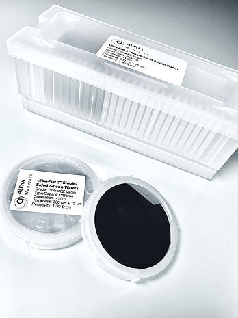 P-type Boron-doped 200nm SiO2 Thermal Oxide Wafer P-type Boron-doped 200nm SiO2 Thermal Oxide Wafer Silicon wafers have been utilized richly in microelectronics and MEMS as a stage for manufacture. A fascinating variety of the standard Diced silicon wafer with a dry oxide coating is the SOI substrate. To deliver these wafers, two silicon wafers are reinforced together, utilizing silicon dioxide of around 1–2 μm thickness as a bond layer. One of the silicon wafers is weakened to a thickness of 10–50 μm. The specific layer thickness will rely upon the application. Wafer diminishing is performed by wet drawing, so this arrangement strategy is frequently called the holding and-etchback method. The covered oxide layer (BOX) isn't available except if mass micromachining is performed, either on the diminished top or full thickness silicon wafer, which likewise goes about as a taking care of stage for preparing. Then again, an uncommon breaking strategy including hydrogen implantation, holding, and warming of the wafer stack to 470°C can be utilized to make a slender silicon wafer on head of the BOX layer. Holding of a 300 μm quartz wafer sandwiched between two standard 525 μm thick silicon wafers was likewise illustrated
These forte substrates discover applications in power gadgets, electronic tasks for application at raised temperatures, mass micromachined xyz-stages, radio recurrence (RF-MEMS) switches, microheater gadgets for microfluidic applications, and coordinated optical frameworks. P-type Boron-doped 200nm SiO2 thermal oxide wafer were submitted to high temperature annealings during long occasions in oxygen and in nitrogen environment so as to recreate similar medicines which are important to create force and high voltage semiconductors or diodes. It is appeared by electrical procedures (microwave distinguished photoconductivity rot and surface photovoltage) and by disclosure methods (checking infrared magnifying lens, X-beam geology, Fourier changed infrared spectroscopy, compound etchings) that annealings in nitrogen added to annealings in oxygen deleteriously affect the lifetime of minority transporters and can make disengagements and accelerates. |
Archives
February 2024
Categories
All
|
 RSS Feed
