|
Quartz moreover has piezoelectric property which is to impart that on the use of a little electric charge, the significant stone vibrates like the treated steel impedance globules. This is the inspiration driving why it is used watches. It what's more has a property known as triboluminescence which interprets that a brightness is passed on when two quartz sorts are scoured out. You can buy quartz stones similarly as the laboratory Prime-grade 4 inch silicon wafer online as indicated by your necessity. It's hard to list the different uses or groupings of quartz significant stones even in a book. Since the old events, quartz has been used in fundamentally all circles of life like fixing, insistence, pearls and various purposes. There is a huge load of captivating emotional information about quartz valuable stone since undeniably the early phase. People of the acclaimed island Diced silicon wafer with a dry oxide coating used to handle the centrality of the sun with huge stones like borosilicate glass contacts. In the Orient, these pearls were cut and used for helping a wide degree of vision issues. 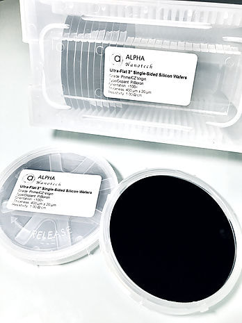 Prime-grade 4 inch silicon wafer Quartz is found in different shapes and sizes on the earth. Purple quartz is known as amethyst while pink quartz is known as rose quartz. Unequivocally when quartz acquires a yellow masking, it known as citrine while dull quartz is known as shake quartz. You can get these materials and besides the Prime-grade 4 inch silicon wafer for lab experimentation online.
Remarkable quartz shock focuses were used by people near the River in 8000 B.C. Formal weapons made out of clear quartz like edges, scrubbers and shot centers were made as old as 700 to 1000 A.D. Diced silicon wafer with a dry oxide coating has been around since the get-go. Regardless the way that we have discovered its uses in science, there is a monstrous load of work to be done as far its extraordinary properties and their astute outcomes are concerned. Click here to know more.
0 Comments
Silicon wafers have been utilized splendidly in microelectronics as well as MEMS as a stage for manufacture. An attractive diversity of the P-type Boron-doped 200nm SiO2 thermal oxide wafer with a dry oxide covering is the SOI substrate. To convey these wafers, two silicon wafers are resistant together, utilizing silicon dioxide of around one to two μm thickness as a bond layer. One of the silicon wafers is destabilized to a thickness of 10–50 μm. The exact layer thickness will depend upon the application. Wafer deteriorating is executed by wet drawing, so this agreement strategy is regularly known as the holding and-etchback process. The enclosed oxide layer (BOX) isn't obtainable except if mass micromachining is executed, either on the diminished top or else complete thickness silicon wafer, which similarly goes about as a taking mind of stage for preparing. Then once more, an infrequent breaking strategy including hydrogen implantation, holding, as well as warming of the wafer stack to 470°C can be utilized to create a slender silicon wafer on head of the BOX layer. 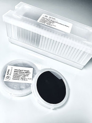 P-type Boron-doped 200nm SiO2 thermal oxide wafer These strong point substrates find applications in power devices; electronic undertakings for application at raised temperatures, mass micromachined xyz-stages, radio repeat (RF-MEMS) switches, microheater devices for microfluidic applications, and facilitated optical structures.
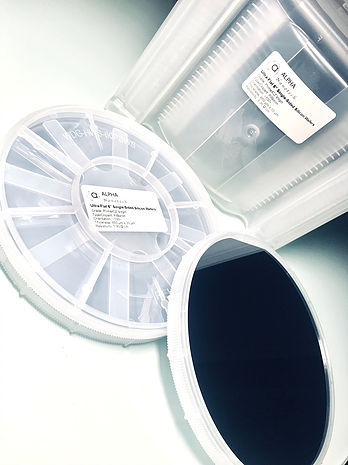
P-type Boron-doped 200nm SiO2 warm oxide wafer were submitted to high temperature annealings during long events in oxygen and in nitrogen climate in order to reproduce comparative prescriptions which are imperative to formulate power along with far above the ground voltage semiconductors or diodes. It is showed up by electrical techniques (microwave recognized photoconductivity decay and surface photovoltage) and by divulgence strategies (checking infrared amplifying focal point, X-bar geography, Fourier changed infrared spectroscopy, compound etchings) that annealings in nitrogen added to annealings in oxygen injuriously influence the lifetime of minority carriers and can make withdrawals and speeds up. Prime-grade 4 inch silicon wafer after cutting have sharp edges, as well as they chip effortlessly. The wafer periphery is shaped to eliminate sharp, brittle edges; rounded edges reduce the peril for slipping, too. The edge shaping process makes the wafer completely round, the diameter is attuned, as well as orientation flat(s) or else notch is dimensioned or made. If the wafer is to be thinned after processing, the wafer edge may, as a consequence be sharp as well as thus brittle utilizing the criterion profile; therefore, an asymmetric edge profile can be utilized. Also, wafer bonding may set precise needs for the wafer edge shape; usually, for bonding applications, a blunter profile is suggested in order to accomplish a good bond up to wafer edge. 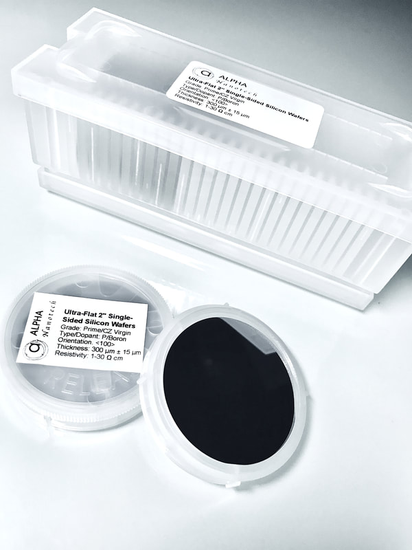 Diced silicon wafer with a dry oxide coating Silicon wafers have been utilized plentifully in microelectronics as well as MEMS as a platform for fabrication. An interesting difference of the pattern silicon wafer is the SOI substrate. To generate these wafers, two silicon wafers are bonded together, utilizing silicon dioxide of roughly 1–2 μm thickness as a bond layer. One of the silicon wafers is insipid down to a breadth of 10–50 μm. The precise layer breadth will depend on the application.
Diced silicon wafer with a dry oxide coating with a dry oxide coating have been utilized expensively in microelectronics as well as MEMS as a phase for produce. An entrancing collection of the criterion Diced silicon wafer with a dry oxide covering is the SOI substrate. To suggest these wafers, two silicon wafers are reinforced together, utilizing silicon dioxide of around 1–2 μm thickness as a bond layer. There is a wide range of applications for which the silicon wafers are used. There are so many electronic items for which these wafers are used to ensure that these devices can work properly and safely. When it comes to the electronic devices, safe operation of these devices is always essential. In case this not happens, then the users of these devices can come across so many issues. In order to keep the operations of these devices safe and smooth, silicon wafers are used. If you are looking for the diced silicon wafer with a dry oxide coating, then you have come to the right place. These silicon wafers come with the coating of dry oxide. That means they are very safe on the use. As far as the electronics like field is concerned, they refer the wafer as the substrate or slice in this field. In this field, these silicon wafers are used to fabricate the integrated circuits. These are also used in the photovolatics field. Here these wafers are used to make the solar cells. P-type Boron-doped 200nm SiO2 thermal oxide wafer
Brand and quality are perhaps the most basic to consider when purchasing required equipment for research focus. Premium models of research office gear with extraordinary operational ampleness are offered by different brands. All these lab devices would separate in their highlights, execution reliable quality and precision of results. It is crucial for pick lab gear that outperforms suspicions in quality from conspicuous creators to profit by astonishing execution and normal quality yield including the Prime-grade 4 inch silicon wafer. Mechanical ends and highlights - It is a remarkable idea to thoroughly review the innovative nuances and highlights of the contraptions that are to be obtained. An appraisal of the various models would assist you with picking restricted equipment and quartz cuvettes got along with design setting progression, and innovative and simple to-utilize highlights. Such lab stuff can suitably meet your particular educational prerequisites of Prime-grade 4 inch silicon wafer. 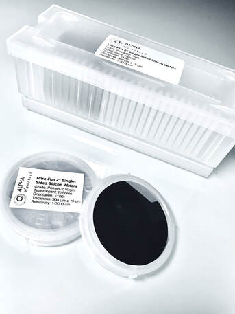 P-type Boron-doped 200nm SiO2 thermal oxide wafer Spending limit - Consider your money related slice off before making capital undertaking for clinical equipment. Amazing devices are a significant part of the time expensive. In the event that you wish to ensure quality contraptions at any rate experience, securing recertified lab machines would be incredible. These contraptions are offered open to be purchased coming about to doing real reconditioning methods and intense appraisal of their show ampleness.
Affirmation choices - Check the confirmation decisions offered for your lab gear including UV vis consolidated fluorescence cuvette. Purchasing devices with acceptable confirmation would assist with settling the operational blemishes anticipating any, correspondingly as affirmation for substitution of parts, or for the gadget in light of everything if there should be an occasion of interminable breakdowns. Nearby these, it is basic to amass relevant data about the clinical research office equipment shippers that offer quality after-bargains organizations. Experienced venders of the lab P-type Boron-doped 200nm SiO2 thermal oxide wafer would give propelling individual help organizations, patch up on the spot yearly assistance contracts, preventive help organization contracts, and in-house organization and fix choices. Solidified silica quartz can also be utilized to make troublesome shapes because of the way that the quartz material has momentous warm deaden obstruction and are unbelievably reliable to most engineered fragments and mixes incorporating Diced silicon wafer with a dry oxide coating. Such a quartz can oversee high assembling of acids and not be affected. The essential dangerous that impacts the Polystyrene nanoparticles would be hydrofluoric ruinous. Truth be told, even in low center this would oppositely impact the material. Stream channel cuvettes conveyed using this material are much of the time utilized for applications, for example, stream cytometry, molecule checking, iota surveying, and different applications. Joined quartz and consolidated Polystyrene microparticles are sorts of glass that are by and large contained silica in its non-clear design. They are conveyed a few novel strategies. The quartz illustrated by warming the material to its molding point and quickly cooling it (called splat-covering or dissolve extinguishing) are suggested as polished. This term is tantamount to utilizing the word glass, for instance glass quartz. P-type Boron-doped 200nm SiO2 thermal oxide wafer Joined quartz or silica is passed on by consolidating high goodness silica in an uncommon radiator. This system is done at incredibly high temperatures, more than 1,000 degrees Fahrenheit.
Conveyed using a high centralization of silicon-rich engineered blends, P-type Boron-doped 200nm SiO2 thermal oxide wafer, made quartz is reliably shaped utilizing a constant fire hydrolysis measure. This strategy joins manufactured gasification of silicon, oxidation of this gas to silicon dioxide, and warm mix of the subsequent development (notwithstanding the path that there are elective frameworks). The result of this procedure is an immediate quartz glass material with a preposterously high flawlessness and the best optical transmission in the huge UV likewise called breath-taking, regardless called the far splendid reach.  Silicon Wafer Silicon Wafer It is probable that most people have come across and even used silicon wafer in their day to day lives. It may not have been deliberate; however, for people who have used devices such as computers and smartphone, they have certainly used this equipment.
Silicon Wafer! What is it? Prime-grade silicon substrate is a material used for producing semiconductors, which can be found in all types of electronic devices that perks up the lives of people. Silicon comes second as the most common element in the universe; it is mostly used as a semi-conductor in the technology and electronic sector. Most individual have had the opportunity to encounter a real silicon wafer in their life. The super-flat desk is refined to a mirror-like surface. It is also made of subtle-surface irregularities which make it the flattest object globally. It is also extremely clean, free of pollutions and micro-particles, qualities that are essential in making it the perfect substrate materials of the contemporary semi-conductors. There are various methods utilized in silicon fabrications counting the horizontal gradient freeze process, vertical Bridgeman method and the pulling method. All through the growth process dopants can be included to amend the purity of the silicon wafer depending on its manufacturing purpose. The pollutants can alter silicon electronic properties which are essential depending on the reason of its production. Some of the silicon dopants that can be added throughout the growth procedure include aluminium, boron, nitrogen, indium, and gallium. A semi-conductor can be regarded as either deteriorates depending on the level the silicon wafer was, when the dopants were added. Visit Alpha Nanotech to obtain supreme quality research material.  Silicon Wafer Silicon Wafer There are many different types of electronic items that we use on a daily basis now. But the fact is we never know that we are also using such an item for the making of which silicon wafer is used. We might have seen the prime-grade silicon substrate several times in our life. But the point is hardly we were able to trace it right. As far as the silicon wafer is concerned, it is an in demand material or element in the electronic and technology like sectors. There is a wide range of electronic items which are made while using this element. You can say that without the use of this element, we cannot even think about the making of the electronic items. And this is what making it the most in demand item now. From computer to the smartphones and other handy devices that we use these days are having semiconductors. These are the most vital components for just any electronic device. When semiconductors are there, you can always expect for a safe use of the electronic device.
 silicon wafer When it comes to the manufacturing of electronic devices, the use of the semiconductors means a lot. In order to get the right kind of semiconductors or to make them, the material like silicon is considered on a high node. This might be a reason why the use of the silicon wafer has managed to draw most attention these days when it comes to the making of the electronic devices. The use of such a wafer as the semiconductor keeps the whole system and further operation of the electronic device safe enough. There are certain complex things associated with electronic devices. However, the use of silicon for these devices is always taken as a simple by the very vital thing. These days, you can find that these wafers are used from making the supercomputers to the android devices and even the microwave ovens. So, this leads us to question why silicon is used and not any other material.
|
Archives
February 2024
Categories
All
|
 RSS Feed
