 SiO2 Thermal Oxide Wafer SiO2 Thermal Oxide Wafer If you are really living in the modern day’s society, then there is always a chance for you to use the silicon wafer knowingly or unknowingly. These items have really managed to bring a revolution in the semiconductor manufacturing sectors. With these wafers, the making of the semiconductors cannot be imagined. So, now you might be thinking that where you have used these items? Well, the answer right at what you are holding in your hand. Yes, it’s the mobile phone or the smartphone that you are using now is such a device for which the silicon wafers are used to keep its use safe for you. The use of these wafers has really made the whole process safer and convenient. Smartphones and computer are the devices that we using on a daily basis. We use these devices to accomplish a wide range of works. But we never know that these devices run so smoothly and safely due to the use of the silicon thermal oxide wafer.
0 Comments
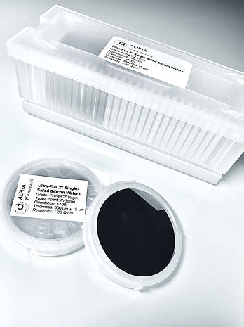 SiO2 Thermal Oxide Wafer SiO2 Thermal Oxide Wafer Produced using a high grouping of silicon-rich synthetic concoctions, manufactured quartz is regularly framed utilizing a progressing fire hydrolysis process. This procedure includes concoction gasification of silicon, oxidation of this gas to silicon dioxide, and warm combination of the subsequent residue (in spite of the fact that there are elective procedures).
The result of this procedure is a straightforward Silicon Thermal Oxide Wafer material with an overly high immaculateness and the best optical transmission in the profound UV otherwise known as ultraviolet, otherwise called the far ultraviolet range. One technique includes adding silicon tetrachloride to a hydrogen-oxygen fire. A hydrogen oxygen fire delivers an exceptionally extreme fire that can without much of a stretch dissolve the quartz and guarantees the quartz combines appropriately. IR grade likewise know as ED-C Quartz is a super immaculateness engineered intertwined silica material. IR Quartz is produced by softening of exceptionally unadulterated cinders in vacuum. It is straightforward in the ultraviolet, unmistakable and infrared ghastly areas. It has no ingestion groups in the obvious district and has no OH retention band at 2700 nm ("water band"). It is realized that laser-initiated debasement antagonistically influences the presentation of intertwined SiO2 thermal oxide wafer optical individuals by diminishing light transmission levels, changing the record of refraction, modifying the thickness, and expanding assimilation levels of the glass. Throughout the years, numerous strategies have been proposed for improving the optical harm obstruction of glass. It has been commonly realized that high virtue quartz material arranged by such techniques as fire hydrolysis, CVD-sediment remelting process, plasma CVD process, electrical intertwining of quartz gem powder, and different strategies, are defenceless to laser harm to different degrees.  SiO2 Thermal Oxide Wafers SiO2 Thermal Oxide Wafers Thermal oxidation is the result of exposing Silicon thermal oxide wafer to a combination of oxidizing agents and heat to make a layer of silicon dioxide. This layer is most commonly made with hydrogen and oxygen gas, although any halogen gas can be utilized.
Silicon dioxide growth takes place on SiO2 thermal oxide wafers in ambient air to about 20 angstroms thick; however, for most specifications thermal oxide growth uses a heat source in order to catalyze this reaction and create oxide layers up to 25000 Angstorms. There are numerous applications for thermal oxidation on silicon wafers, and both require growth of oxygen on the surface of the water. This differs from CVD applications, where the oxide layer is deposited on top of the wafer. Growth rate of silicon thermal oxide wafer The preliminary growth of the oxide is limited by the rate at which the chemical retort takes place. After the first 100 to 300 Angstroms of oxide has been produced, the growth rate of oxide layer will be limited principally by the rate of diffusion of the oxidant through the oxide layers. Specifications
SiO2 Thermal Oxide Wafer There is a wide range of applications for which the silicon wafer is used. But before you use this element, you always need to know that how it is made or from what source it is extracted. And while trying to analyze these elements, you may come across the fact that silicon is the material which is very common in this universe is also located on our earth. This material is also considered as the mostly found material in this universe and it plays a very vital role in the universe as well. So, now the silicon thermal oxide wafer is announced for the market and the prime source for it is the silicon that we can observe on our earth now. There is a wide range of industries where this element is needed. It also used for a wide range of applications. When you are looking at the use of this element, you can also find that it is also used in the fields like electronic and technology.
|
Archives
February 2024
Categories
All
|
 RSS Feed
